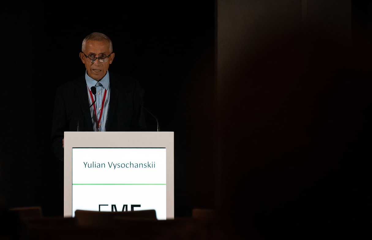
Physics without borders: an interview with Professor Julian Vysochanskyi about international scientific projects.

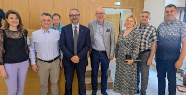
Cooperation with scientific institutions in the USA, Switzerland, France, and Spain is a common practice for the Physics Department of UzhNU. For a long time now, they have been working on projects that allow the university to maintain its high scientific position. Such international contacts contribute to raising the scientific level of the department and establishing the university's authority in the world. One of the people directly responsible for these achievements is Julian Vysochansky, academician of the National Academy of Sciences of Ukraine, Doctor of Physical and Mathematical Sciences, professor, and head of the Department of Semiconductor Physics. We spoke with him about an international project, which will be two years old in October, entitled “Piezoelectricity in 2D Materials: Materials, Modeling, and Applications.” The research conducted within the framework of the project will form the basis for future developments in nanoscale electronic devices for decades to come.Cooperation with scientific institutions in the USA, Switzerland, France, and Spain is a common practice for the Physics Department of UzhNU. For a long time now, they have been working on projects that allow the university to maintain its high scientific position. Such international contacts contribute to raising the scientific level of the department and establishing the university's authority in the world. One of the people directly responsible for these achievements is Julian Vysochansky, academician of the National Academy of Sciences of Ukraine, Doctor of Physical and Mathematical Sciences, professor, and head of the Department of Semiconductor Physics. We spoke with him about an international project, which will be two years old in October, entitled “Piezoelectricity in 2D Materials: Materials, Modeling, and Applications.” The research conducted within the framework of the project will form the basis for future developments in nanoscale electronic devices for decades to come. One of the series of such collaborations is the submission of applications for experiments. For example, structural studies at very high pressures. So we traveled with colleagues to Hamburg, where the German Electron Synchrotron (DESY) is located, whose base allows high-precision research to be carried out using synchrotron radiation.
We also conducted research with colleagues at the Laue-Langevin Institute (ILL) in Grenoble, and at the Léon Brillouin Laboratory (LLB) in Saclay (France), in Geneva (Switzerland) at CERN, the European Organization for Nuclear Research. Our work looks like this: we request an experiment, a panel considers whether it is appropriate to allocate time, resources, and equipment for the research, and only then is our request approved.
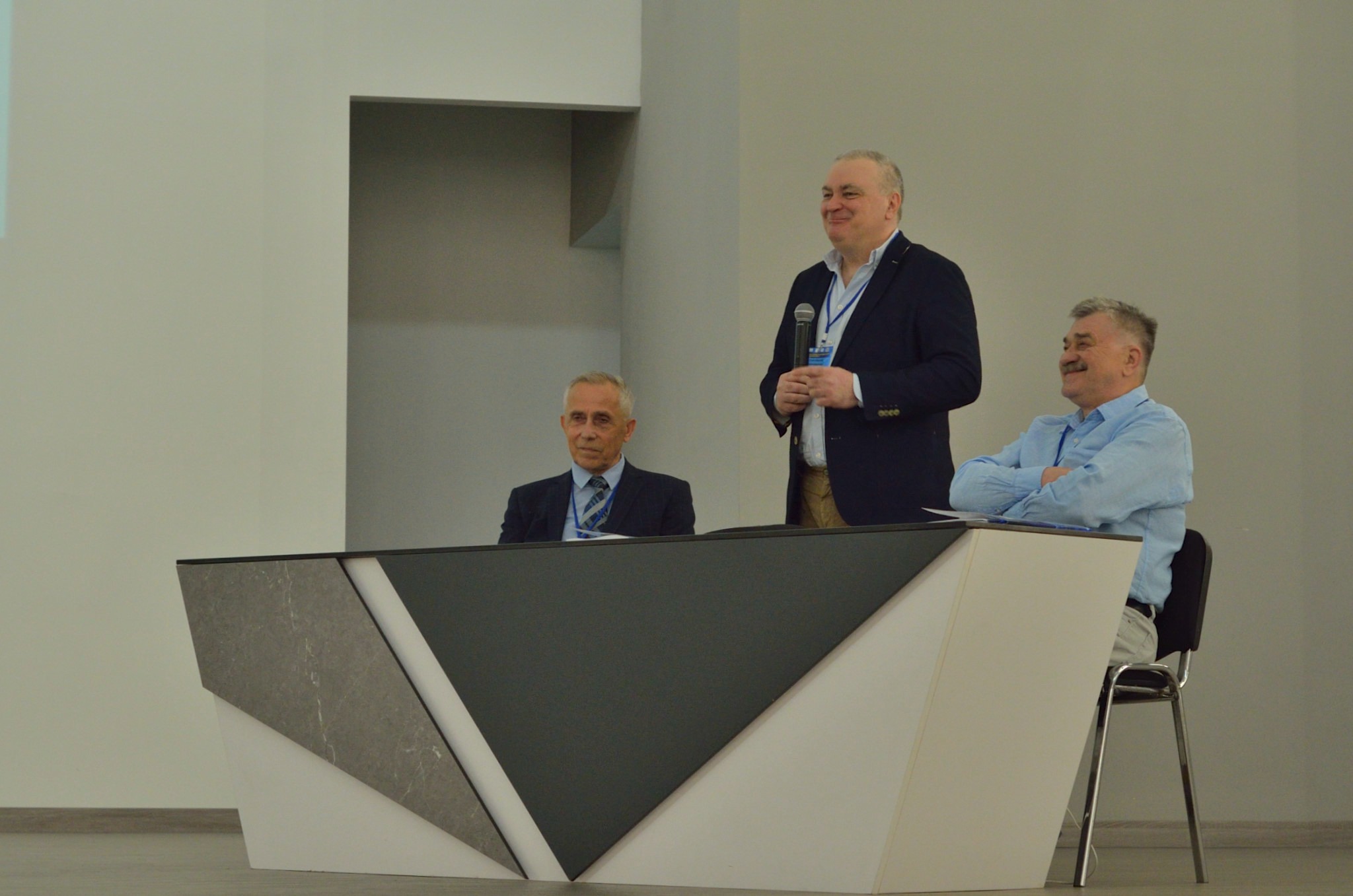
So, once again, we gathered at an international conference on ferroelectricity physics, which was held in Tel Aviv. My colleagues and I had a conversation during which we agreed to try to organize a project in a specific area of research, namely layered materials, the thickness of which can be reduced to a single layer of atoms by exfoliation, and to observe the switching of the direction of spontaneous polarization by an electric field. When the polarization vector orientation changes, the sign of the sample deformation changes due to the piezoelectric effect. These are the so-called electromechanical effects. Such properties are very important for modern electronics because they allow the creation of ferroelectric diodes, transistors, and electronic analogues of synapses, i.e., the imitation of neuromorphic calculations that reproduce the computing process characteristic of the human brain. Based on these materials, it is also possible to create machine vision systems, and we already have a co-authored publication on this topic. These are advanced technologies in nanoelectronics that are used in various fields of science, technology, engineering, and for special purposes as well.
So this agreement has yielded results—when the European Commission announced its next competition under the Horizon Europe program, we decided to submit our application. Namely: Uzhhorod National University, the Institute of Physics of the National Academy of Sciences of Ukraine, the University of Aveiro (Portugal), the University of Bilbao (Spain), the Technical University of Denmark, and the Institute of Low Temperature and Structural Research of the Polish Academy of Sciences (Wrocław, Poland).
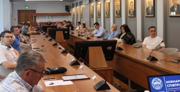
We worked on this project for about a year, it was evaluated, received a passing score, and was successfully approved. We signed a fairly extensive agreement with the European Commission. And so, the project began. In October this year, it will be two years old. We had an introductory meeting in Wrocław, and a working meeting in Aveiro. During the implementation of the project, it was decided to involve the Institute of Physics of the University of Riga.
This May, a working meeting was also held in Riga with the participation of representatives of the European Commission. We are already preparing our report for the two-year period of the project. We are constantly posting information about the progress of the project on the European Commission's website. In addition, we maintain the project's own website, where we post materials about our meetings, scientific seminars, publications, and abstracts of reports.
Within the framework of the project, working trips are regularly organized to gain new experiences. In particular, I have already been to Portugal and Poland, and visits to Denmark and Spain are also planned. We hope to receive a positive assessment, as funding has been allocated for two years (these are the conditions for the implementation of the project). If the evaluation is positive, the European Commission will continue funding for the next two years.
— Why is this area important and relevant for the physics community right now?
— Information technology is the basis of almost all areas of activity, from education, medicine, logistics, and communications to social... According to estimates, due to the enormous amount of information processed by data centers, the energy consumed by existing computer technologies will exceed the energy consumed by industry, the utilities sector, and transportation on a global scale in the coming years.
This means that it is now a pressing task to reduce the energy consumption of computing systems, all these servers and processors that handle Internet traffic, calculations, etc. We are talking about classic computers, not quantum computers, which will also be widely used in the future.
Reducing energy consumption can be achieved by reducing the size and increasing the density of functional elements, transistors. Previously, diodes or transistors were about five millimeters in size — you could open the board, replace something, or re-solder it. Then came microelectronics, where we are talking about fractions of a millimeter, hundredths of a millimeter. And later came nanoelectronics. In particular, heterostructures made of atomic monolayers. So it turns out that our materials are very effective components for creating nanoscale functional heterostructures. We have a good base at the department, as well as at the Institute of Chemistry and Ecology of UzhNU in terms of materials production technologies, and this also applies to the base for optical and electrophysical research. We use the equipment of the UzhNU Center for Collective Use of Scientific Equipment. However, as I mentioned, for the application of synchrotron radiation or neutron beams, we naturally draw on the research capabilities of international centers, particularly in Grenoble and Hamburg. We have been conducting joint research with CERN for about five years. Incidentally, UzhNU is one of the four leading Ukrainian scientific institutions that cooperate with CERN. So there are certain experiments for which the resources of international centers are used. Each scientific center has specific scientific complexes for advanced research. We are talking about highly specialized equipment – an electron beam accelerator, a high-energy charged particle accelerator. We also cooperate with the University of Zurich, with which we recently started a parallel project led by Professor Oleksandr Hrabar.